Contact Information:

Professor Yao-Jen Lee
Ph.D. in Electrical Engineering from National Chiao Tung University
Adjunct Research Fellow at Taiwan Semiconductor Research Institute
Primary Email:yjlee1976@gmail.edu.tw
School Email:yjlee1976@nycu.edu.tw
Office: Room 371, Engineering Building 6 (EF-371)
TEL: +886-3-71-2121 ext.58526
Laboratory: Room 453, Engineering Building 6 (EF-453)
TEL: +886-3-71-2121 ext.58520
Introduction of ASD Lab.:
This research team is led by Dr. Yao-Jen Lee, who has served at the Taiwan Semiconductor Research Institute (TSRI)for over sixteen years and continues to hold a concurrent position as a research fellow there. The team members come from several major universities in Taiwan, and most of the research work is conducted at TSRI and the National Yang Ming Chiao Tung University (NYCU) Nano Facility Center. For specialized or advanced process modules, the team also collaborates with international research institutions, including the National Institute of Advanced Industrial Science and Technology (AIST)in Japan.
Graduate students in this laboratory receive comprehensive training on a full-scale device fabrication platform and participate in the development and implementation of cutting-edge devices. Graduates possess solid skills in semiconductor processing and device integration, and most go on to work for leading technology companies in Taiwan and abroad.
State-of-the-art research platform:
Our research is primarily conducted at two top-tier facilities—TSRI and NYCU Nano Facility Center. The lab is equipped with ALD systems,Small-scale CMP, low-power plasma tools, and a complete measurement environment. Device characterization across a wide temperature range—from cryogenic (4 K) to high temperature (150 °C)—can be performed within our lab. Students gain hands-on experience operating industry-grade advanced equipment, turning innovative research ideas into reality.
Efficient learning and knowledge transfer system:
No need to start from scratch! Thanks to the efforts of previous members, we have established a mature “Advanced Device Fabrication Platform.” This systematic process significantly shortens the learning curve, enabling new students to quickly engage in core research and focus on the development and innovation of advanced devices.
Our laboratory focuses on key technologies in the post-Moore’s Law era and is organized into three core research teams exploring future transistor device possibilities:
1.Vertical Transistor Integration Team (VFET Integration Team)
Focused on the structural design, process development, and electrical characterization of vertical-channel transistors (Vertical FETs).
2.Polysilicon/Silicon/Germanium Channel Device Integration Team(Ge FinFET/GAA/CFET Team)
Centered on germanium-based channels (Ge channel), this team studies the integration technologies of advanced nano-devices such as FinFET, GAA, and CFET.
3.Oxide Semiconductor (OS) GAA/CFETs Integration Team
Dedicated to the device applications of oxide semiconductor (OS) materials, exploring their potential and process compatibility within GAA and CFET architectures.
Recent research results:
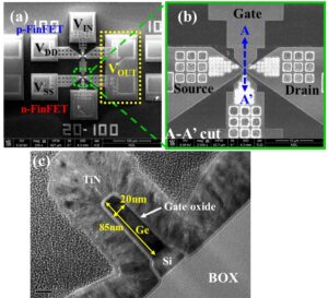
Fig1. Ge FinFETs Platform: Ge CMOS platform, fabricated on the Ge epitaxial layer on SOI, is used to study Ge properties from the prospectives of finFETs.
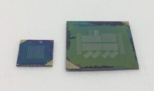
Fig2. From 8-Inch Wafers to Wafer Dicing:Transitioning from 8-inch wafers to wafer dicing processes not only reduces device fabrication costs but also enhances the flexibility of our research.
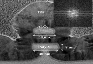
Fig3. Polysilicon Stacked CMOS Platform
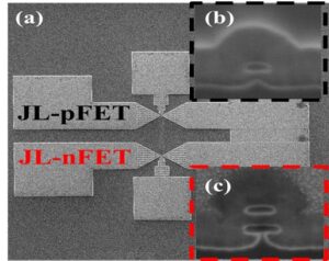
Fig4. Polysilicon Stacked CMOS Platform
The polysilicon stacked CMOS platform allows for adjusting the channel count for pFET and nFET using photolithography and etching processes.
- Varying the channel count promotes the current balance.
- Why is there one less channel in pFET? Because the threshold voltage leans towards nFET.
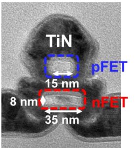
Fig5. Complementary FET (CFET) Platform, Presented at IEDM 2019
- The pFET appears narrower due to the longer etching time.
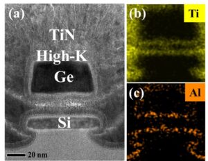
Fig6. Heterogeneous Integration of Ge/Si CFET Platform.
- In collaboration with AIST Japan, our team utilizes a low-temperature bonding process to bond Ge and Si, forming heterogeneous integrated CFET devices.
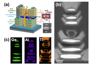
Fig7. (a) 3D schematics of Ge CFET. (b) TEM image and (c) EDS mapping result of Ge CFET.
- Our team has successfully fabricated a six-channel Ge CFET (three pFET layers and three nFET layers) through epitaxyand low-temperature bonding techniques. This achievement has been accepted for publication in IEEE Electron Device Letters (EDL).
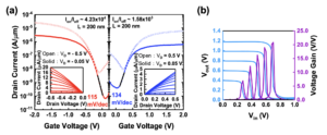
Fig8.(a) The measured transfer, output and (b) CMOS characteristics of Ge CFET.